16-bit RISC-based CPU
Winter 2024
Overview
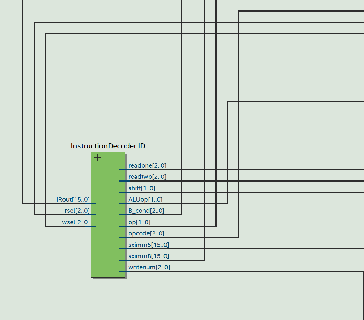
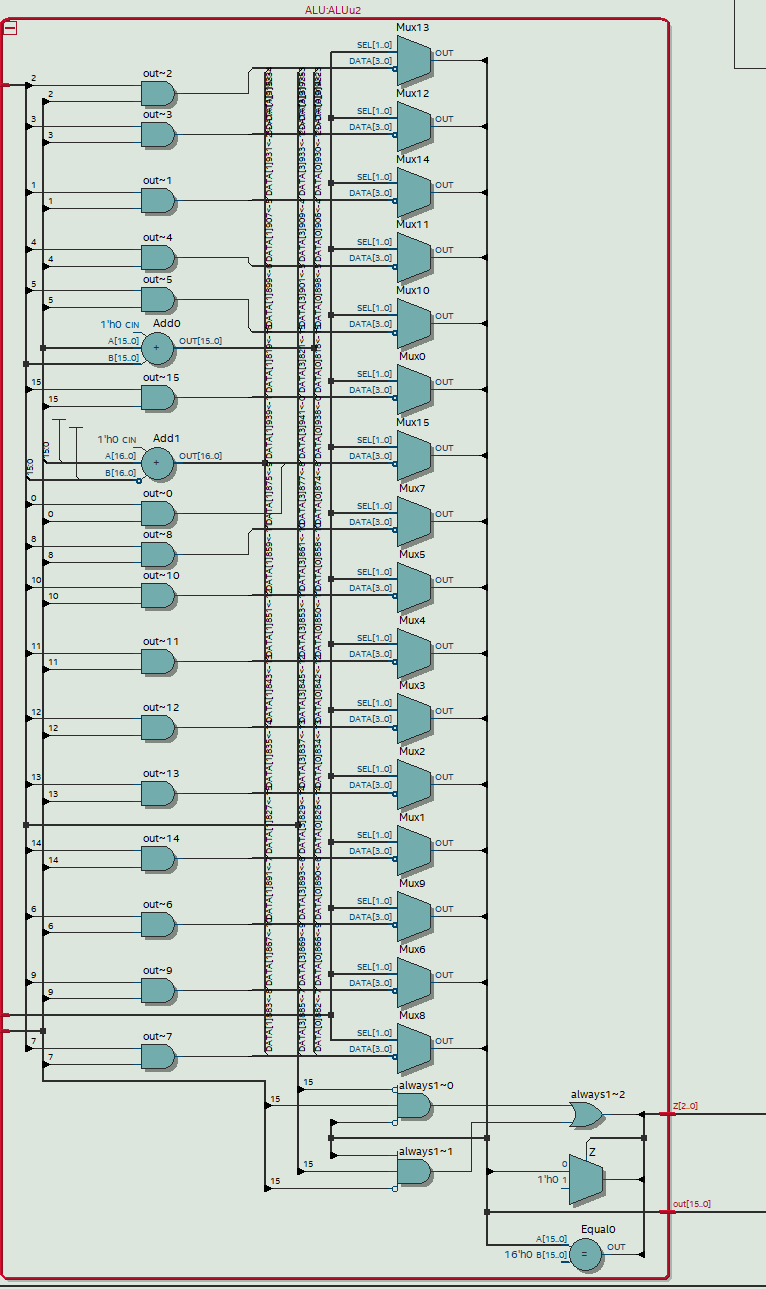
I see you are a connoisseur of RISC based computer architecture aren't you? This project involved designing and implementing a 16-bit RISC-style CPU in Verilog, then simulating and testing it on an Altera DE1-SoC FPGA board. The design followed a a standard 5 stage fetch–decode–execute-memory-writeback cycle (yeah I sort of paid attention in my classes), with a state-machine controller directing the flow of execution. This controller interpreted the outputs of the instruction decoder module and generated the appropriate control signals to drive the ALU and memory.
While 16 bits does limit your instruction set a tad we were going for RISC anyways so it ended up being planty.
The instruction set included all the usual suspects: arithmetic (ADD,SUB), logic (AND,MVN,CMP),
data movement (MOV), memory access (LDR,STR) and branch instrucitons (B,BEQ,BNE,BLT,BLE).
The ALU module carried out arithmetic and logical operations, while a dedicated block of RAM provided program memory and data storage.
The load/store capability made it possible to execute small test programs and observe the CPU’s behavior directly on the FPGA hardware.
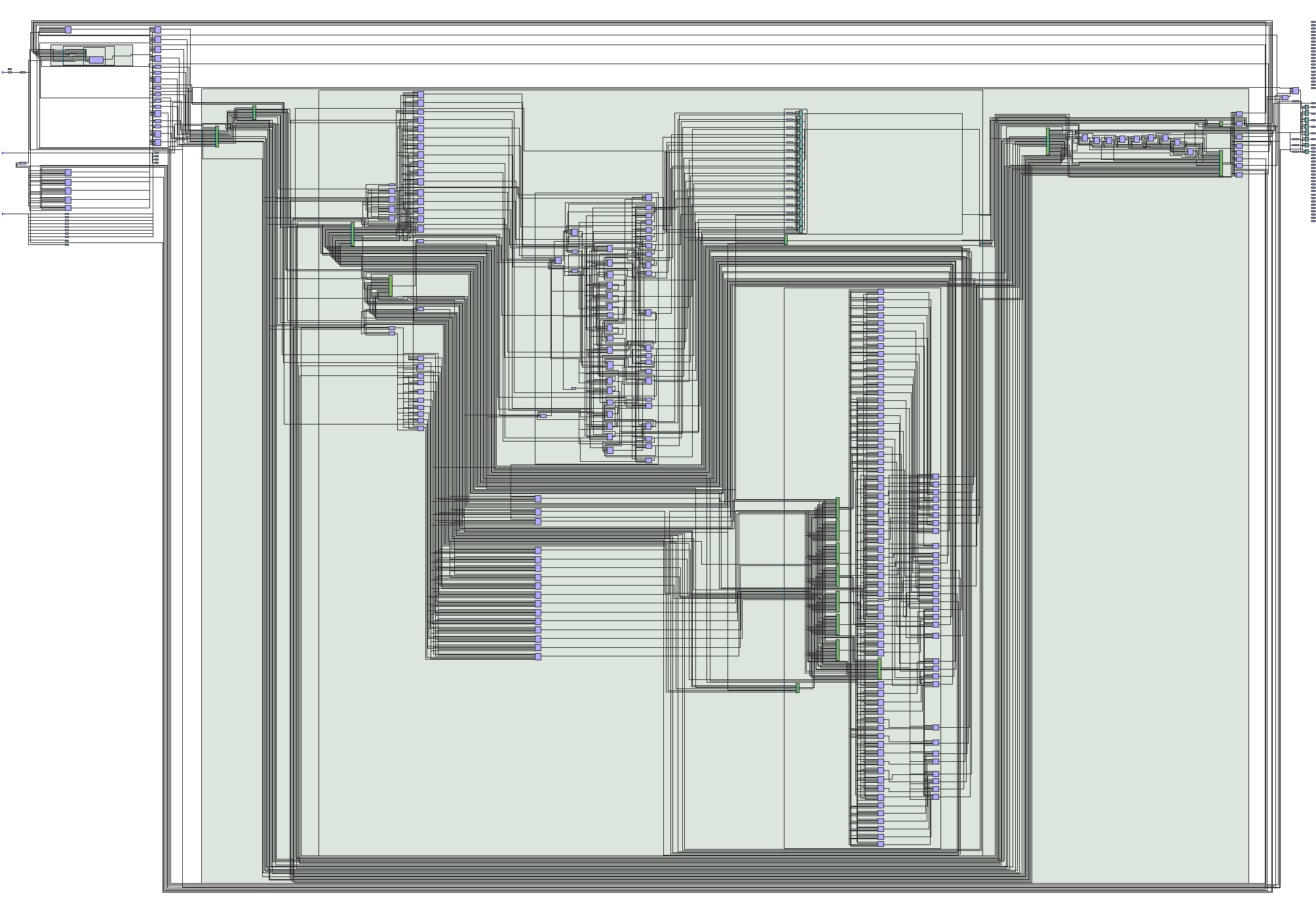
To bring everything together, the top-level CPU design (shown below) connected the instruction decoder, ALU, and memory into the datapath. I learned so much about about risc architecture and FPGA simulation over the course of this project. Hopefully going forward I'd like to learn more about branch prediction to improve pipelining (AI in branch prediction seems awesome). This project also got me super interested in exploring superscalar architecture as well as vector processors like GPU design.
Key Features
- Word size: 16-bit
- Platform: Altera DE1-SoC FPGA
- Language: Verilog